 Ken K.H. Leung, Testing Engineer, Google
But some of the products they’re meant to protect have changed. At Google, where fully assembled data center racks weighing thousands of pounds are shipped around the world, that mismatch is becoming impossible to ignore.
“The supply chain is completely complicated,” says Ken Leung, who has spent 15 years leading shock and vibration testing for Google’s data center hardware. “You may have servers that are built in Asia… racks built in America… integrated somewhere else… and then shipped again.”
The goal is to be able to roll a fully populated rack off a truck, plug it in at the destination data center, and turn it on. But the journey there introduces a set of sustained movement (shock and vibration) variables that packaging engineers might know well, but may still underestimate.
Movement is the failure mechanism
In Leung’s framing, vibration and shock are the root cause of failure.
“When you’re shipping these things around the world, that vibration… is going to cause things to move relative to each other,” he explains.
That movement happens at every level of the system—from materials and components to racks, packaging, vehicles, and terrain, as illustrated in Google’s presentation stack diagram
 Google’s Ken Leung frames shock and vibration as a system-level challenge, spanning components, racks, packaging, vehicles, and real-world transport conditions. Ken Leung, Google
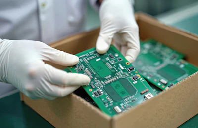
The problem is especially acute in modern electronics. As AI-driven hardware becomes smaller, denser, and more powerful, its mechanical durability often declines. The below slide from Leung’s presentation summarizes the tradeoff. Faster signals, smaller components, and higher power all contribute to “weaker structure” and reduced mechanical durability. This is true of consumer products like TVs, computers, and cell phones, too. For packaging engineers who have to design packaging for these products, the margin for error is shrinking. As electronics become smaller, faster, and more powerful, their mechanical durability often declines—tightening tolerances for packaging and transport.Ken Leung, Google
The failure you don’t see is the one that matters
One of the most counterintuitive insights from Leung’s work is that immediate failure is preferable.
“You’re lucky if it doesn’t turn on,” he says of a newly delivered system.
If a unit fails at startup, the issue is obvious and diagnosable. The real risk lies in damage that occurs during transport but doesn’t show up right away.
In his presentation, Leung describes how solder joints can crack under shock, then reconnect when the system returns to a neutral position, allowing the product to pass initial testing.  Shock damage can be invisible at first—fractured connections may temporarily recover, only to fail later in operation.Ken Leung, Google
“The damage is already done,” the slide notes, leading to “intermittent and long-term reliability issues.”
Weeks or months later, under thermal cycling and operational stress, those microfractures can lead to failure, sometimes during critical operations. In large-scale AI environments, that can mean lost compute time, retraining cycles, and significant cost.
Why traditional testing falls short
Despite these risks, most testing methods still rely on indirect measurement.
“Most people don’t really know physically what’s happening to the real product,” Leung says.
Accelerometers and shaker tables generate large volumes of data, but they don’t show how internal components within a package (especially products with lots of componentry that's connected together) actually move. As a result, engineers often default to trial-and-error solutions.
“Put more foam in it… put more materials in it,” Leung says. “And actually sometimes that makes it worse.”
In one example, adding soft foam increased internal motion, allowing heavy components like heat sinks to oscillate more (like bobble-head dolls, he joked) amplifying stress rather than reducing it.
The issue isn’t lack of testing, rather it's lack of visibility into what's really happening to a product inside of a package, and how a package dampens (or doesn't) shock and vibration.
A shift from measurement to visualization
Leung’s work centers on changing that. By combining high-speed cameras, computer vision, and multi-angle imaging, his team can now observe internal motion directly and track how specific components bend, shift, and interact under vibration. High-speed imaging and computer vision allow engineers to visualize how components actually move during vibration—revealing failure points that traditional sensors miss.Ken Leung, Google
“Suddenly it gave me all these things… all kinds of craziness that’s going on,” he says of early motion-amplified video experiments.
Leung is doing most of his AI vision work on RDI Technology's RDI Motion Amplification cameras, though they aren't the only product in the field. Using multiple cameras, the system can reconstruct true 3D displacement of individual points on a board, allowing engineers to identify exactly where stress concentrates.
“I don’t have to look at everything on the board anymore,” Leung says. “I can focus on where the most movement, causing the biggest problems, is happening and solve the problems there.”
That shift from broad testing to targeted investigation is the real breakthrough.
Rather than testing repeatedly and reinforcing packaging after failures occur, engineers can identify the specific components or regions at risk and address them directly. 3D measurement reveals where movement (and risk) is concentrated, allowing engineers to focus design and packaging improvements on critical areas.
From hyperscale hardware to everyday packaging
At first glance, Google’s data center hardware, with its tight tolerances and high value, may seem far removed from consumer packaged goods. But Leung thinks the underlying physics is the same, so it should be relatable.
“Materials and stress is universal,” he says. “Whether it’s… a computer server or nuts and bolts that hold together consumer products… it’s all going to translate.”
The difference is not in the principles, but in the margin.
For many CPG products, structures are robust enough that vibration rarely leads to catastrophic failure. But the same forces of movement, stress, and fatigue are still present. And without clear visibility, packaging decisions are often made conservatively or iteratively.
That leads to a familiar cycle: test, observe failure, add material, test again. The alternative is a more data-driven approach: understand how the product actually behaves, then design packaging around those insights.
“It beats trying to do a test… and then you try to beef from the foam again… you never really get anywhere. For every new product, you have to start from scratch,” Leung said.
Building a shared body of knowledge
To accelerate that shift, Leung is releasing its methods through an open-source project, including field data, lab replication techniques, and measurement approaches. The project lives in GitHub, and is available here: https://github.com/GoogleCloudPlatform/open-random-vibration-testing-of-ots-dc-hardware
The goal is to make advanced testing capabilities more accessible—not just to large organizations, but to suppliers, test labs, and even students.
“If you guys have tools and an infrastructure to do this,” Leung says, “it would be a lot easier… not having to create or come up with things from scratch.”
That accessibility is key. While few organizations will replicate Google’s full testing infrastructure, the broader lesson is not about scale—it’s about mindset.
The next evolution of packaging engineering
As products become more complex across industries—from electronics to medical devices to smart packaging—the need for deeper understanding of physical behavior is only increasing.
Leung’s advice to packaging engineers is straightforward: focus on the fundamentals, and embrace collaboration.
“Physics is universal… it's the ultimate limiter to all this stuff,” he says.
But no single engineer or organization can tackle the complexity alone.
“These things are incredibly complex… learning to work together… that’s what we need to do.”
In that sense, the shift toward AI-driven visualization isn’t just a new tool. It represents a broader evolution—from testing packaging as an external shell to understanding it as part of a dynamic system.
For engineers willing to look inside the case, it may finally break the cycle of trial and error that has defined the field for decades.